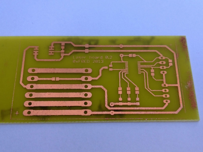
Board Etching
To avoid the need of exposing the board it is possible to transfer laser printed layouts
directly.
First print the layout on a glossy magazin paper. Thin paper should first fixed on a normal
sheet of paper to avoid problems during printing. The layout must be mirrored.
Cut the board to the desired size, as well as the printed layout. Try not to touch the
printed surface with the fingers, handle the paper by the edges. Clean the copper side of
the board throughly using ultra fine sand paper or metal wool and rub with pure acetone.
Now you can put together the printed paper and the board.
Place a cold regular clothing iron in top of the paper side. The iron temperature SHOULD
be set at around 120 Celsius not too much colder or hotter (in my iron it is the SILK setting,
or between the NYLON and POLYESTER settings). The idea is only to make the toner in the print
soft and sticky, but not to melt it down. With the iron in place turn it on and,
without moving, just apply pressure till it reaches the temperature setting. I then start
moving the iron in circles applying gentle pressure for three to five minutes. At the end
you will notice the circuit design through the paper. Turn off the iron and let the PCB
cool down for a while.
Once cool, place the PCB in a tray with water. After just a few minutes you will notice
that the paper turns loose and the toner has transfered completely to the copper.
There is no need to rub the paper to remove it. The PCB is then ready for the chemical treatment.